- 您现在的位置:买卖IC网 > Sheet目录307 > ADP3611JRMZ-REEL (ON Semiconductor)IC MOSFET DRIVER DUAL 10-MSOP
�� �
�
�ADP3611�
�IN�
�DRVLSD�
�0.8� V�
�t� pdlDRVLSD�
�2.0� V�
�t� pdhDRVLSD�
�DRVL�
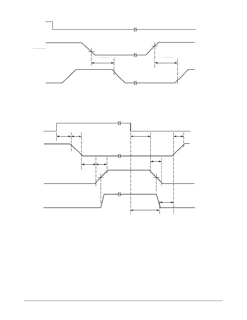
�Figure� 3.� Output� Disable� Timing� Diagram� (Timing� is� Referenced� to�
�the� 90%� and� 10%� Points� Unless� Otherwise� Noted)�
�IN�
�DRVL�
�t� pdlDRVL� t� fDRVL�
�t� pdlDRVH�
�t� rDRVL�
�DRVH� ?� SW�
�t� pdhDRVH�
�t� rDRVH�
�V� TH�
�t� fDRVH�
�V� TH�
�SW�
�1V�
�t� pdhDRVL�
�≤� t� SWTO�
�Figure� 4.� Nonoverlap� Timing� Diagram� (Timing� is� Referenced� to� the�
�90%� and� 10%� Points� Unless� Otherwise� Noted)�
�http://onsemi.com�
�4�
�发布紧急采购,3分钟左右您将得到回复。
相关PDF资料
ADP5501ACPZ-RL
IC LED DRVR WHITE BCKLGT 24LFCSP
ADP8863ACPZ-R7
IC LED DRVR WHIT BCKLGT 20-WLCSP
ADUM1100UR
IC DIGITAL ISOL/COUPLER 8SOIC
ADUM1201CR
IC ISOLATOR DIGITAL DUAL 8SOIC
ADUM1210BRZ
IC ISOLATOR DIGITAL DUAL 8SOIC
ADUM1233BRWZ-RL
IC ISOLATR DGTL 2CH 0.1A 16-SOIC
ADUM1234BRWZ-RL
IC ISOLATR DGTL 2CH 0.1A 16-SOIC
ADUM1250SRZ-RL7
IC ISOLATOR 1MBPS 4CH 2.5K 8SOIC
相关代理商/技术参数
ADP3611MNR2G
功能描述:功率驱动器IC DUAL HI VOLT MOSFET RoHS:否 制造商:Micrel 产品:MOSFET Gate Drivers 类型:Low Cost High or Low Side MOSFET Driver 上升时间: 下降时间: 电源电压-最大:30 V 电源电压-最小:2.75 V 电源电流: 最大功率耗散: 最大工作温度:+ 85 C 安装风格:SMD/SMT 封装 / 箱体:SOIC-8 封装:Tube
ADP3611MNR2G-REEL
制造商:ONSEMI 制造商全称:ON Semiconductor 功能描述:Dual Bootstrapped, High Voltage MOSFET Driver with Output Disable
ADP3623
制造商:AD 制造商全称:Analog Devices 功能描述:High Speed, Dual, 4 A MOSFET Driver with Thermal Protection
ADP3623ARDZ-RL
功能描述:IC MOSFET DVR 4A DL HS 8SOIC RoHS:是 类别:集成电路 (IC) >> PMIC - MOSFET,电桥驱动器 - 外部开关 系列:- 标准包装:95 系列:- 配置:高端和低端,独立 输入类型:非反相 延迟时间:160ns 电流 - 峰:290mA 配置数:1 输出数:2 高端电压 - 最大(自引导启动):600V 电源电压:10 V ~ 20 V 工作温度:-40°C ~ 125°C 安装类型:表面贴装 封装/外壳:8-SOIC(0.154",3.90mm 宽) 供应商设备封装:8-SOIC 包装:管件 产品目录页面:1381 (CN2011-ZH PDF)
ADP3623ARHZ-RL
功能描述:IC MOSFET DVR 4A DL HS 8MSOP RoHS:是 类别:集成电路 (IC) >> PMIC - MOSFET,电桥驱动器 - 外部开关 系列:- 标准包装:95 系列:- 配置:高端和低端,独立 输入类型:非反相 延迟时间:160ns 电流 - 峰:290mA 配置数:1 输出数:2 高端电压 - 最大(自引导启动):600V 电源电压:10 V ~ 20 V 工作温度:-40°C ~ 125°C 安装类型:表面贴装 封装/外壳:8-SOIC(0.154",3.90mm 宽) 供应商设备封装:8-SOIC 包装:管件 产品目录页面:1381 (CN2011-ZH PDF)
ADP3624
制造商:AD 制造商全称:Analog Devices 功能描述:High Speed, Dual, 4 A MOSFET Driver with Thermal Protection
ADP3624ARDZ
功能描述:IC DRIVER DUAL 4A NONINV 8SOIC RoHS:是 类别:集成电路 (IC) >> PMIC - MOSFET,电桥驱动器 - 外部开关 系列:- 标准包装:95 系列:- 配置:半桥 输入类型:PWM 延迟时间:25ns 电流 - 峰:1.6A 配置数:1 输出数:2 高端电压 - 最大(自引导启动):118V 电源电压:9 V ~ 14 V 工作温度:-40°C ~ 125°C 安装类型:表面贴装 封装/外壳:8-SOIC(0.154",3.90mm 宽) 供应商设备封装:8-SOIC 包装:管件 产品目录页面:1282 (CN2011-ZH PDF) 其它名称:*LM5104M*LM5104M/NOPBLM5104M
ADP3624ARDZ-RL
功能描述:IC DVR DUAL NONINVERT 4A 8SOIC RoHS:是 类别:集成电路 (IC) >> PMIC - MOSFET,电桥驱动器 - 外部开关 系列:- 标准包装:50 系列:- 配置:低端 输入类型:非反相 延迟时间:40ns 电流 - 峰:9A 配置数:1 输出数:1 高端电压 - 最大(自引导启动):- 电源电压:4.5 V ~ 35 V 工作温度:-40°C ~ 125°C 安装类型:表面贴装 封装/外壳:TO-263-6,D²Pak(5 引线+接片),TO-263BA 供应商设备封装:TO-263 包装:管件